We must explain to you how all seds this mistakens idea denouncing pleasures and praising account.

At Intrinsic SoC Solutions, we provide comprehensive FPGA verification services to ensure the functionality and reliability of your FPGA design. Our experienced verification engineers use industry-standard tools and methodologies to thoroughly test and verify your FPGA design, reducing the risk of errors and improving overall quality.
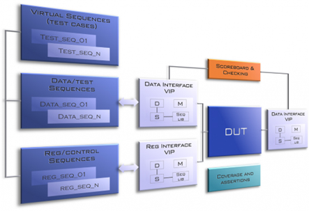
Our FPGA verification process typically involves the following steps:
Test plan development: We work closely with you to develop a test plan that covers all functional and non-functional requirements of your FPGA design.
Testbench development: We create a testbench that emulates the environment in which your FPGA will operate, including stimuli generation, monitoring, and checking.
Testcase development: We develop testcases based on the test plan and the testbench, using various verification techniques such as directed testing, random testing, and coverage-driven testing.
Simulation and debugging: We simulate the design using industry-standard simulation tools and debug any issues that arise during the simulation.
Formal verification: We use formal verification techniques such as model checking and theorem proving to exhaustively verify specific properties of the design.
Emulation and prototyping: We can also perform FPGA verification using emulation and prototyping techniques to speed up the verification process and test the design in a more realistic environment.

Address: No154/20, Third Floor T-1,
Royal Space, 5th
Main, 174-HSR Layout 7th Sector,
Madina Nagar, Bommanahalli,
Bangalore -560102
Phone:+91 7259457618X
Email: hr@Intrinsicsoc.com
Intrinsic SoC Solutions - Copyright 2023. All rights reserved.
Designed and Developed By Sapiosolutions